
CoolSiC™ MOSFETs Generation 2
Empowering the next generation of high-performance systems
Empowering the next generation of high-performance systems
Explore how the new CoolSiC™ MOSFET G2 trench MOSFET enables a new level of SiC performance, while meeting the highest quality standards in all common combinations of power schemes: AC-DC, DC-DC and DC-AC. Photovoltaic inverters, energy storage systems, EV charging, power supplies, motor drives and more belong to the many cases where SiC MOSFETs provide additional performance, compared to Si alternatives.
Features:
- 400 V / 650 V / 1200 V CoolSiC MOSFET G2
- Lowest available RDS(on)
- Largest product portfolio
- Unique robustness features
Energy efficiency for every Watt of power processed
Power losses matter. Explore how the new CoolSiC™ MOSFET G2 trench technology improves on power delivery in common topologies used in AC/DC, DC/DC, DC/AC power schemes. Key figures-of-merit for both, hard-switching and soft-switching MOSFET operation, are improved by more than 20% compared to the previous generation. The fast switching capability, i.e. the signature of SiC MOSFETs, is in addition improved by more than 30%. As a result, G2 operates with lower power losses in all operation modes in photovoltaic inverters, energy storage installations, EV charging, UPS and more. With the example of three-phase power schemes, compared to the previous generation 1200 V CoolSiC™ G2 operates at 5-30% lower power losses depending on the load condition, enabling energy savings for every Watt processed in the field.
Further advancement of Infineon´s unique .XT interconnection technology (e.g. in discrete housings TO-263-7, TO-247-4) serves to overcome the common challenge of improving semiconductor chip performance while maintaining its thermal capability. The thermal capability is now 12% better for the new generation, boosting the chip figures-of-merit to a new level of SiC performance.
Raising the bar for the power possible in a given form factor
Combining the best of SiC: low power losses in small form factors. The lower is the on-resistance of a SiC MOSFET, the lower are the conduction losses, allowing more energy efficiency, power density and part count reduction. CoolSiC™ G2 MOSFET portfolios boost the lowest Rdson in the SiC MOSFET market. The introduction of best in class products in SMD packages, makes 7 mOhm rating in 650 V and 8 mOhm rating in 1200 V available in TO263-7 form factor. Improved package interconnect with .XT results in less thermal resistance, more output power, lower operating temperature. The power that can be delivered by an SMD form factor is increased by more than 60%, and raises the bar for power density possible in power conversion schemes.
Setting a new standard for utilization of SiC performance
Maximizing each Euro invested in SiC. Explore a series of new robustness features in CoolSiC™ MOSFET G2 products for reaching the best performance during long-term field operation. The system designer can now benefit from a datasheet specification of maximum on-resistance at 150°C in 1200 V portfolios. The SiC MOSFET capability can be fully utilized when no additional margins due to uncertainty of distributions must be accounted for at elevated temperatures during nominal operation. Overload operation up to a virtual junction temperature of 200°C is included in 1200 V CoolSiC™ MOSFET G2 datasheets and introduced first in the TO-263-7 package. For coping with overload events coming from e.g. grid fluctuations, the system designer can design for higher output currents compared to the previous generation, or reduce on cooling efforts. The specified avalanche robustness on datasheet level further eases the system design effort for such over-current events. A strong immunity against unwanted turn-on events, a rugged body diode operation during hard commutation, and short-circuit capability are supported by datasheet specifications in CoolSiC™ MOSFET G2 products.
CoolSiC™ is another great example for Infineon´s quality leadership
All modern Silicon power devices are trench based and have replaced the planar technologies so what about Silicon Carbide? For SiC, there are many similarities with the Silicon power MOSFET technology evolution when it comes to performance advantages by trench design. One more striking advantage comes in addition with trench design in SiC, namely reliability. Vertical interfaces show significantly lower defect density compared to lateral ones in SiC material. This opens up a new optimization potential for matching performance and robustness features with reliability. Reliability is the fundament of every power device development at Infineon and CoolSiC™ MOSFET G2 trench technology maintains the high G1 reliability. DPM (defects per million) data based on all CoolSiC™ MOSFETs G1 sold, discretes and modules industrial grade, shows that product returns for SiC are even below silicon based power switches, a very mature technology. Infineon has also pioneered in application lifetime testing and certain tests are nowadays included in the JEDEC standard. The CoolSiC™ trench MOSFET design drives sustainable competitiveness for energy efficiency, now and in the future
Infineon’s CoolSiC™ product categories: Find your best fitting products
Infineon continuously added SiC-based products - including the revolutionary CoolSiC™ MOSFETs in trench technology - to the already existing Si-assortment. Today the company offers one of the most comprehensive power portfolios in the industry – ranging from ultra-low to high-voltage power devices. Going even beyond only ensuring the availability of best-fit solutions, we walked the extra mile to optimize the SiC-based product offering to meet specific application requirements.
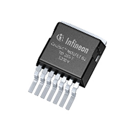
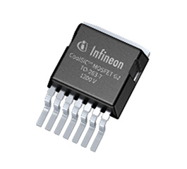
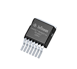
CoolSiC™ MOSFET 1200 V G2
The CoolSiC™ MOSFET 1200 V, 26 mΩ G2 in a D2PAK-7L (TO-263-7) package builds on the strengths of Generation 1 technology and enables the accelerated system design of more cost optimized, efficient, compact, and reliable solutions. Generation 2 comes with significant improvements in key figures-of-merit for both, hard-switching operation and soft-switching topologies, suitable for all common combinations of AC-DC, DC-DC, and DC-AC stages.
| Part number | Specification | Package | Applications |
|---|---|---|---|
 IMBG120R026M2H | CoolSiC™ MOSFET 1200 V G2 | TO-263-7 |
|
 IMBG120R234M2H | CoolSiC™ MOSFET 1200 V G2 | TO-263-7 |
|
 IMBG120R008M2H | CoolSiC™ MOSFET 1200 V G2 | TO-263-7 |
|
 IMBG120R053M2H | CoolSiC™ MOSFET 1200 V G2 | TO-263-7 |
|
 IMBG120R017M2H | CoolSiC™ MOSFET 1200 V G2 | TO-263-7 |
|
 IMBG120R116M2H | CoolSiC™ MOSFET 1200 V G2 | TO-263-7 |
|
 IMBG120R012M2H | CoolSiC™ MOSFET 1200 V G2 | TO-263-7 |
|
 IMBG120R181M2H | CoolSiC™ MOSFET 1200 V G2 | TO-263-7 |
|
 IMBG120R078M2H | CoolSiC™ MOSFET 1200 V G2 | TO-263-7 |
|
 IMBG120R040M2H | CoolSiC™ MOSFET 1200 V G2 | TO-263-7 |
|
 IMBG120R022M2H | CoolSiC™ MOSFET 1200 V G2 | TO-263-7 |
|
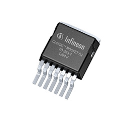
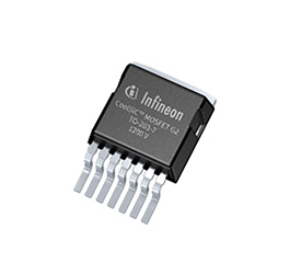
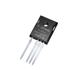
The CoolSiC™ MOSFET 650 V, 20 mΩ G2 in a TO-247-3
package builds on the strengths of Generation 1 technology and enables the accelerated system design of more cost optimized, efficient, compact, and reliable solutions. Generation 2 comes with significant improvements in key figures-of-merit for both, hard-switching operation and soft-switching topologies, suitable for all common combinations of AC-DC, DC-DC, and DC-AC stages.
| Part number | Specification | Package | Applications |
|---|---|---|---|
 IMW65R020M2H | CoolSiC™ MOSFET 650 V | PG-TO247-3 |
|
 IMZA65R020M2H | CoolSiC™ MOSFET 650 V | PG-TO247-4 |
|
 IMZA65R040M2H | CoolSiC™ MOSFET 650 V | PG-TO247-4 |
|
 IMBG65R015M2H | CoolSiC™ MOSFET 650 V G2 | PG-TO263-7 |
|
 IMBG65R007M2H | CoolSiC™ MOSFET 650 V G2 | PG-TO263-7 |
|
 IMBG65R040M2H | CoolSiC™ MOSFET 650 V G2 | PG-TO263-7 |
|
 IMBG65R020M2H | CoolSiC™ MOSFET 650 V G2 | PG-TO263-7 |
|
 IMBG65R050M2H | CoolSiC™ MOSFET 650 V G2 | PG-TO263-7 |
|
 IMZA65R050M2H | CoolSiC™ MOSFET 650 V G2 | PG-TO247-4 |
|
IMZA65R050M2H | CoolSiC™ MOSFET 650 V G2 | PG-TO247-4 |
|
 IMW65R050M2H | CoolSiC™ MOSFET 650 V G2 | PG-TO247-3 |
|
 IMW65R040M2H | CoolSiC™ MOSFET 650 V G2 | PG-TO247-3 |
|
 IMW65R015M2H | CoolSiC™ MOSFET 650 V G2 | PG-TO247-3 |
|
Videos
CoolSiC™ discrete MOSFET Generation 2
Power conversion solutions that guarantee high energy efficiency are key to reaching decarbonization goals and achieving unlimited green energy. SiC based power electronics boost energy efficiency compared to Si alternatives in many cases. To speed up the implementation of clean energy and energy efficiency in a global world Infineon is releasing the second generation of CoolSiC™ MOSFETs.
Introducing Infineon CoolSiC™ MOSFET discrete 650 V G2
Be familiar with Infineon's CoolSiC™ MOSFET discrete 650 V generation 2, know its key features, target application and benefits and understand its positioning compared to other technologies.
CoolSiC™ MOSFET 第 2 代
为下一代高性能系统赋能
为下一代高性能系统赋能
了解新型 CoolSiC™ MOSFET G2 沟槽式 MOSFET 如何让 SiC 的性能更上一层楼,同时满足所有常见电源方案组合(交流-直流、直流-直流和直流-交流)的最高质量标准。与同类型的 Si 产品相比,SiC MOSFET 在光伏逆变器、储能系统、电动汽车充电、电源、电机驱动器等众多案例中都能提供更出色的性能。
特色:
- 400 V / 650 V / 1200 V CoolSiC MOSFET G2
- 最低可提供的 RDS(on)
- 最大规模的产品组合
- 独特的耐用特性
处理每瓦特功率的能源效率
电力损耗很重要。 探索新型 CoolSiC™ MOSFET G2 沟槽技术如何改善交流/直流、直流/直流和直流/交流电源方案中常用拓扑结构的电力传输。 与上一代产品相比,硬开关和软开关 MOSFET 操作的关键品质因数都提高了 20% 以上。 此外,快速开关能力(即 SiC MOSFET 的特征)提高了 30% 以上。 因此,G2 在光伏逆变器、储能装置、电动汽车充电和 UPS 等的所有运行模式下都以较低的功率损耗运行。 以三相电源方案为例,与上一代相比,1200 V CoolSiC™ G2 运行时功率损耗降低 5-30%,具体视负载条件而定,处理每一瓦特功率都能节省能源。
进一步推进 Infineon 独特的 .XT 互连技术(例如,在分立式封装 TO-263-7、TO-247-4 中),用于克服在保持其热性能的同时,提高半导体芯片性能的双重挑战。 现在,新一代的热性能提高了 12 %,将芯片的品质因数提升到了 SiC 性能的新水平。
提高了给定外形尺寸下的功率标准
结合了 SiC 的优点:尺寸小巧、功率损耗低。 SiC MOSFET 的导通电阻越低,导通损耗就越低,从而能够获得更高的能效和功率密度,以及更少部件数量。 CoolSiC™ G2 MOSFET 产品组合提高了 SiC MOSFET 市场中的最低 Rdson。 在 SMD 封装中引入最好的同类产品,使得在 TO263-7 的外形尺寸下可以做到在 650 V 时的额定值为 7 mOhm,1200 V 时的额定值为 8 mOhm。 改进的 .XT 封装互连可降低热阻,提高输出功率,降低运行温度。 SMD 外形尺寸可提供的功率增加达 60 % 以上,并提高了电源转换方案中可能的功率密度标准。
为 SiC 性能利用设定新标准
充分发挥投资于 SiC 的每一欧元的作用。探索 CoolSiC™ MOSFET G2 产品的各种全新耐用特性,从而在长期运行过程中实现最佳性能。 系统设计人员现在可以从 1200 V 产品组合中 150°C 下最大导通电阻的数据表规范中受益。 高温下正常运行时,由于不需要考虑分布不确定性而产生的额外裕量,SiC MOSFET 的性能可以得到充分利用。 1200 V CoolSiC™ MOSFET G2 可在虚拟结温高达 200°C 的情况下过载运行,并在 TO-263-7 封装中首次引入。 为了应对电网波动情况等带来的过载事件,系统设计者在设计阶段可以采用比上一代产品更高的输出电流,或减少为冷却而做的工作。 数据表级别的指定雪崩稳定性进一步简化了针对此类过流事件的系统设计工作。 根据 CoolSiC™ MOSFET G2 产品的数据表,它具备应对意外导通事件的出色抗扰度、在硬换向期间可靠的体二极管运行,以及短路能力。
CoolSiC™是 Infineon 以质量取胜的又一典范
所有现代的硅功率器件均基于沟槽,并且已经取代了平面技术,那么碳化硅呢? 对于 SiC 而言,在沟槽设计的性能优势方面,它与硅功率 MOSFET 技术的发展有许多相似之处。 此外,SiC 中的沟槽设计还有一个更显著的优势,那就是可靠性。 与 SiC 材料的横向面相比,垂直面的缺陷密度明显更低。 这为将性能和稳定性特性与可靠性相匹配提供了新的优化潜力。 可靠性是 Infineon 每一款功率器件开发的基础,而 CoolSiC™ MOSFET G2 沟槽技术同样继承了 G1 的高可靠性。 基于所有已售出的 CoolSiC™ MOSFET G1、分立器件和工业级模块的 DPM(每百万分件的缺陷数量)数据显示,SiC 的产品退货率甚至比采用硅基功率开关这一非常成熟技术的产品还要低。 Infineon 在应用寿命测试方面也处于领先地位,某些测试目前已被纳入 JEDEC 标准。 CoolSiC™ 沟槽式 MOSFET 设计推动了现在和未来能源效率的可持续竞争力
Infineon 的 CoolSiC™ 产品类别:找到最适合您的产品
除了现有基于 Si 的产品,Infineon 还在不断增加基于 SiC 的产品,包括采用突破性沟槽技术的 CoolSiC™ MOSFET。 如今,该公司提供了业内最全面的电力产品组合之一,从超低压到高压电力设备,一应俱全。 除了确保提供最适合的解决方案之外,我们还进一步优化了基于 SiC 的产品,以满足特定的应用要求。
CoolSiC™ MOSFET 1200 V G2
The CoolSiC™ MOSFET 1200 V, 26 mΩ G2 in a D2PAK-7L (TO-263-7) package builds on the strengths of Generation 1 technology and enables the accelerated system design of more cost optimized, efficient, compact, and reliable solutions. Generation 2 comes with significant improvements in key figures-of-merit for both, hard-switching operation and soft-switching topologies, suitable for all common combinations of AC-DC, DC-DC, and DC-AC stages.
| Part number | Specification | Package | Applications |
|---|---|---|---|
IMBG120R026M2H | CoolSiC™ MOSFET 1200 V G2 | TO-263-7 |
|
IMBG120R234M2H | CoolSiC™ MOSFET 1200 V G2 | TO-263-7 |
|
IMBG120R008M2H | CoolSiC™ MOSFET 1200 V G2 | TO-263-7 |
|
IMBG120R053M2H | CoolSiC™ MOSFET 1200 V G2 | TO-263-7 |
|
IMBG120R017M2H | CoolSiC™ MOSFET 1200 V G2 | TO-263-7 |
|
IMBG120R116M2H | CoolSiC™ MOSFET 1200 V G2 | TO-263-7 |
|
IMBG120R012M2H | CoolSiC™ MOSFET 1200 V G2 | TO-263-7 |
|
IMBG120R181M2H | CoolSiC™ MOSFET 1200 V G2 | TO-263-7 |
|
IMBG120R078M2H | CoolSiC™ MOSFET 1200 V G2 | TO-263-7 |
|
IMBG120R040M2H | CoolSiC™ MOSFET 1200 V G2 | TO-263-7 |
|
IMBG120R022M2H | CoolSiC™ MOSFET 1200 V G2 | TO-263-7 |
|
The CoolSiC™ MOSFET 650 V, 20 mΩ G2 in a TO-247-3
package builds on the strengths of Generation 1 technology and enables the accelerated system design of more cost optimized, efficient, compact, and reliable solutions. Generation 2 comes with significant improvements in key figures-of-merit for both, hard-switching operation and soft-switching topologies, suitable for all common combinations of AC-DC, DC-DC, and DC-AC stages.
| Part number | Specification | Package | Applications |
|---|---|---|---|
IMW65R020M2H | CoolSiC™ MOSFET 650 V | PG-TO247-3 |
|
IMZA65R020M2H | CoolSiC™ MOSFET 650 V | PG-TO247-4 |
|
IMZA65R040M2H | CoolSiC™ MOSFET 650 V | PG-TO247-4 |
|
IMBG65R015M2H | CoolSiC™ MOSFET 650 V G2 | PG-TO263-7 |
|
IMBG65R007M2H | CoolSiC™ MOSFET 650 V G2 | PG-TO263-7 |
|
IMBG65R040M2H | CoolSiC™ MOSFET 650 V G2 | PG-TO263-7 |
|
IMBG65R020M2H | CoolSiC™ MOSFET 650 V G2 | PG-TO263-7 |
|
IMBG65R050M2H | CoolSiC™ MOSFET 650 V G2 | PG-TO263-7 |
|
IMZA65R050M2H | CoolSiC™ MOSFET 650 V G2 | PG-TO247-4 |
|
IMZA65R050M2H | CoolSiC™ MOSFET 650 V G2 | PG-TO247-4 |
|
IMW65R050M2H | CoolSiC™ MOSFET 650 V G2 | PG-TO247-3 |
|
IMW65R040M2H | CoolSiC™ MOSFET 650 V G2 | PG-TO247-3 |
|
IMW65R015M2H | CoolSiC™ MOSFET 650 V G2 | PG-TO247-3 |
|
视频
CoolSiC™ 分立式 MOSFET 第 2 代
高能效的电源转换解决方案是实现减排目标和实现无限绿色能源的关键。 在许多情况下,与 Si 同类产品相比,基于 SiC 的电力电子设备具有更高的能源效率。 为了加快清洁能源在全球的推广实施,并提高能源效率,Infineon 发布了第二代 CoolSiC™ MOSFET。
Infineon CoolSiC™ MOSFET 分立器件 650 V G2 简介
熟悉 Infineon 的 CoolSiC™ MOSFET 分立器件 650 V 第 2 代,了解其主要特性、目标应用和优势,并通过与其他技术进行比较,了解该产品的定位。