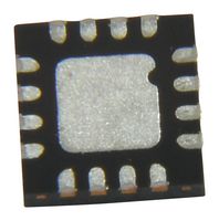
ADCLK925BCPZ-R7
Clock & Data Buffer IC, 2.375 V to 3.63 V, 7.5 GHz, 2 Outputs, LFCSP-16, -40°C to 125°C

Need more?
| Quantity | Price (inc GST) |
|---|---|
| 10+ | CNY85.500 (CNY96.615) |
| 25+ | CNY75.950 (CNY85.8235) |
| 100+ | CNY65.500 (CNY74.015) |
| 250+ | CNY64.190 (CNY72.5347) |
| 1500+ | CNY62.880 (CNY71.0544) |
Product Information
Product Overview
ADCLK925 (one input, two outputs) is an ultrafast clock/data buffer fabricated on the Analog Devices, Inc., proprietary XFCB3 silicon germanium (SiGe) bipolar process. It feature full-swing emitter coupled logic (ECL) output drivers. For PECL (positive ECL) operation, bias VCC to the positive supply and VEE to ground. For NECL (negative ECL) operation, bias VCC to ground and VEE to the negative supply. The inputs have centre tapped, 100 ohm, on-chip termination resistors. A VREF pin is available for biasing ac-coupled inputs. The ECL output stages are designed to directly drive 800mV each side into 50 ohm terminated to VCC − 2V for a total differential output swing of 1.6V. It is widely used in application such as clock and data signal restoration and level shifting, automated test equipment (ATE), high speed instrumentation, high speed line receivers, threshold detection, converter clocking etc.
- Propagation delay is 95ps typical
- Toggle rate is 7.5GHz typical
- Random jitter is 60fs rms typical
- On-chip terminations at both input pins
- Power supply range is 2.5V to 3.3V
- Input bias current is 20µA typical
- Operating temperature is -40°C to +125°C
- Package style is 16-lead lead frame chip scale package [LFCSP]
Notes
ADI products are only authorized (and sold) for use by the customer and are not to be resold or otherwise passed on to any third party
Technical Specifications
Clock & Data Buffer
2Outputs
3.63V
16Pins
125°C
-
No SVHC (21-Jan-2025)
7.5GHz
2.375V
LFCSP-EP
-40°C
-
MSL 3 - 168 hours
Technical Docs (1)
Legislation and Environmental
Country in which last significant manufacturing process was carried outCountry of Origin:Philippines
Country in which last significant manufacturing process was carried out
RoHS
RoHS
Product Compliance Certificate