S25FS512SDSBHV213
闪存, 串行NOR, 512 Mbit, 64M x 8位, SPI, BGA, 24 引脚

产品信息
产品概述
S25FS512SDSBHV213 is a 512Mb FS-S flash memory. This connects to a host system via a serial peripheral interface. Traditional SPI single bit serial input and output is supported as well as optional two-bit (Dual I/O or DIO) and four-bit wide Quad I/O (QIO) or quad peripheral interface serial commands. This multiple-width interface is called SPI Multi-I/O or MIO. In addition, there are double data rate (DDR) read commands for QIO and QPI that transfer address and read data on both edges of the clock. The FS-S Eclipse architecture features a Page Programming Buffer that allows up to 512bytes to be programmed in one operation, resulting in faster effective programming and erase than prior generation SPI program or erase algorithms. By using S25FS512S devices at the higher clock rates supported, with Quad or DDR-Quad commands, the instruction read transfer rate can match or exceed traditional parallel interface, asynchronous, NOR flash memories, while reducing signal count dramatically.
- 80MHz DDR speed, 1.7V to 2.0V supply voltage range
- Serial peripheral interface (SPI) with multi-I/O, SPI clock polarity and phase modes 0 and 3
- Serial command subset and footprint compatible with S25FL-A, S25FL-K, S25FL-P, S25FL-S SPI families
- Multi I/O command subset and footprint compatible with S25FL-P, and S25FL-S SPI families
- Normal, fast, dual I/O, quad I/O, DDR quad I/O commands, burst wrap, continuous (XIP), QPI modes
- Serial flash discoverable parameters and common flash interface for configuration information
- Program suspend and resume
- Erase suspend and resume, erase status evaluation
- 100,000 program-erase cycles (minimum), 20 year data retention (minimum)
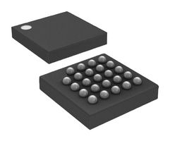
- 24-ball BGA package, industrial plus temperature range from -40°C to +105°C
技术规格
串行NOR
512Mbit
64M x 8位
SPI
BGA
80MHz
-
2V
表面安装
105°C
MSL 3 - 168小时
512Mbit
64M x 8位
SPI
BGA
24引脚
80MHz
1.7V
1.8V
-40°C
1.8V Serial NOR Flash Memories
No SVHC (25-Jun-2025)
技术文档 (1)
法律与环境
进行最后一道重要生产流程所在的地区原产地:Thailand
进行最后一道重要生产流程所在的地区
RoHS
RoHS
产品合规证书