ADCLK905BCPZ-R7
时钟/数据缓冲器,7.5GHz,1 输出,3.63V,LFCSP-EP-16,-40°C 至 125°C

需要更多?
| 数量 | 价钱 (含税) |
|---|---|
| 1+ | CNY108.820 (CNY122.9666) |
| 10+ | CNY75.580 (CNY85.4054) |
| 25+ | CNY66.930 (CNY75.6309) |
| 100+ | CNY57.150 (CNY64.5795) |
| 250+ | CNY56.230 (CNY63.5399) |
| 500+ | CNY55.110 (CNY62.2743) |
| 1500+ | CNY53.990 (CNY61.0087) |
产品信息
产品概述
ADCLK905 is a one input, one output, ultrafast clock/data buffer fabricated on the Analog Devices, Inc., proprietary XFCB3 silicon germanium (SiGe) bipolar process. It features full-swing emitter coupled logic (ECL) output drivers. For PECL (positive ECL) operation, bias VCC to the positive supply and VEE to ground. For NECL (negative ECL) operation, bias VCC to ground and VEE to the negative supply. The buffers offer 95ps propagation delay, 7.5GHz toggle rate, 10Gbps data rate, and 60fs random jitter (RJ). The inputs have centre tapped, 100 ohm, on-chip termination resistors. A VREF pin is available for biasing ac-coupled inputs. It is used in applications such as clock and data signal restoration and level shifting, automated test equipment (ATE), high speed instrumentation, high speed line receivers, threshold detection, converter clocking.
- 2.5V to 3.3V power supply (VCC − VEE)
- On-chip terminations at both input pins
- Output rise/fall time is 60ps typical
- Power supply rejection ratio is 3ps/V typical at (VCC − VEE = 3V ± 20%)
- Output resistance is 250 ohm typical
- Input bias current is 20µA typical
- Input capacitance is 0.4pF typical
- Operating temperature is -40°C to +125°C
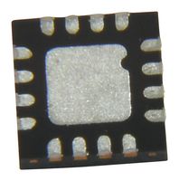
- Package style is 16-lead LFCSP
注释
ADI products are only authorized (and sold) for use by the customer and are not to be resold or otherwise passed on to any third party
技术规格
时钟/数据缓冲器
1输出
3.63V
16引脚
125°C
-
No SVHC (21-Jan-2025)
7.5GHz
2.375V
LFCSP-EP
-40°C
-
MSL 3 - 168小时
技术文档 (1)
法律与环境
进行最后一道重要生产流程所在的地区原产地:Philippines
进行最后一道重要生产流程所在的地区
RoHS
RoHS
产品合规证书